本文翻译自 jaycarlson 的 blog: So you want to build an embedded Linux system?
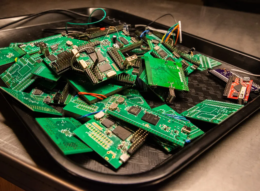
我的办公室在过去的几个月里完全被这些小型的 Linux 板子淹没了——我总共发了超过 25 块板子, 测试 DDR 布线规则、电源架构, 并修复了一些 bug.
Processor vendors vigorously encourage reference design modification and reuse for customer designs. I think most professional engineers are most concerned with getting Rev A hardware that boots up than playing around with optimization, so many custom Linux boards I see are spitting images of off-the-shelf EVKs.
处理器供应商积极鼓励对参考设计的修改和重用. 我认为大多数专业工程师最关心的是获得能够启动的样板, 而不是玩优化, 所以我看到的许多定制 Linux 板都是现成 EVK (evaluation kit, 评估板) 的复制品.
But depending on the complexity of your project, this can become downright absurd. If you need the massive amount of RAM that some EVKs come with, and your design uses the same sorts of large parallel display and camera interfaces, audio codecs, and networking interfaces on the EVK, then it may be reasonable to use this as your base with little modification. However, using a 10-layer stack-up on your simple IoT gateway — just because that’s what the ref design used — is probably not something I’d throw in my portfolio to reflect a shining moment of ingenuity.
但是, 根据你项目的复杂性, 这可能会变得相当荒谬. 如果你需要某些 EVK 所配备的大量 RAM, 并且你的设计使用了相同类型的大型并行显示器和摄像头接口、音频编解码器和网络接口, 那么使用这个作为基础, 进行少量修改可能是合理的. 然而, 仅仅因为参考设计使用了 10 层板, 就在你的简单物联网网关上使用它——反正我是不会将它当作一个闪光的创新时刻放入我的作品集的.
People forget that these EVKs are built at substantially higher volumes than prototype hardware is; I often have to explain to inexperienced project managers why it’s going to cost nearly $4000 to manufacture 5 prototypes of something you can buy for $56 each .
大家常常忘记这些 EVK 的产量比你的样板高得多;我经常不得不向缺乏经验的项目经理解释, 为什么打 5 个样板会花费近 4000 美元 , 而你只需支付 56 美元 就可以购买一个.
You may discover that it’s worth the extra time to clean up the design a bit, simplify your stackup, and reduce your BOM — or just start from scratch. All of the boards I built up for this review were designed in a few days and easily hand-assembled with low-cost hot-plate / hot-air / pencil soldering in a few hours onto cheap 4-layer PCBs from JLC . Even including the cost of assembly labor, it would be hard to spend more than a few hundred bucks on a round of prototypes so long as your design doesn’t have a ton of extraneous circuitry.
你可能会发现, 花点额外时间整理一下设计、减少叠层、减少 BOM 或者干脆从头开始是有价值的. 我为此评测搭建的所有电路板都是在几天内设计的, 并且可以轻松手焊, 在嘉立创的廉价 4 层 PCB 上下单, 之后使用低成本的加热台/热风枪/电烙铁焊接几个小时就可以了. 即使包括组装人工成本, 只要你的电路板设计没有大量多余的电路, 一轮打样的成本也很难超过几百美元.
If you’re just going to copy the reference design files, the nitty-gritty details won’t be important. But if you’re going to start designing from-scratch boards around these parts, you’re going to notice some major differences from designing around microcontrollers.
如果你只是复制参考设计文件, 细节问题并不重要. 但如果你要从这些部件开始从头设计电路板, 你会注意到与微控制器相关设计的一些重大差异.
BGA Packages #
BGA (ball grid array, 球栅阵列) 封装
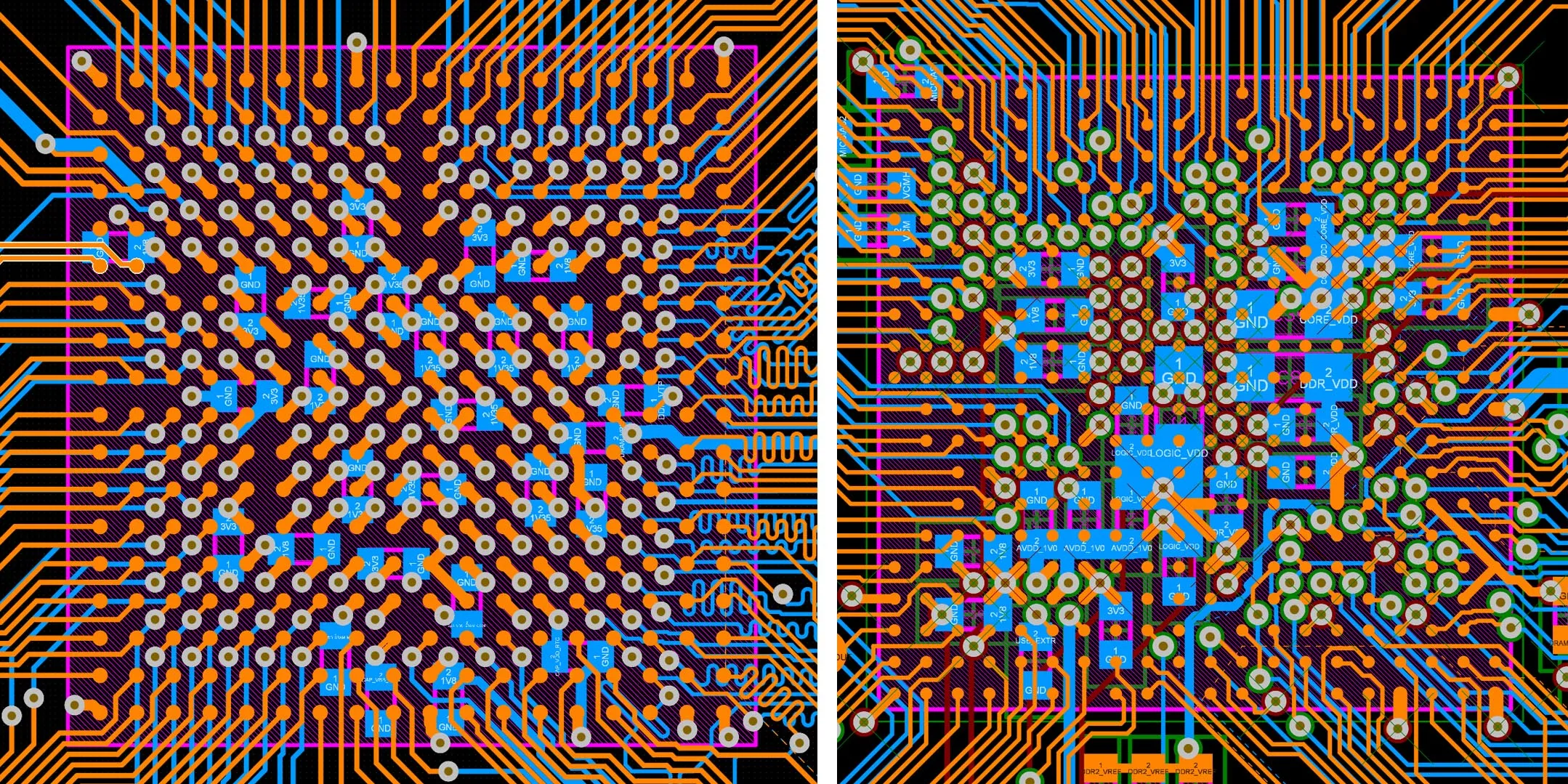
德州仪器的 AM335x (左侧) 具有完整的 0.8mm 间距球栅阵列;而瑞芯微的 RK3308 (右侧) 则采用了选择性去除的 0.65mm 间距球栅阵列.
Most of the parts in this review come in BGA packages, so we should talk a little bit about this. These seem to make less-experienced engineers nervous — both during layout and prototype assembly. As you would expect, more-experienced engineers are more than happy to gatekeep and discourage less-experienced engineers from using these parts, but actually, I think BGAs are much easier to design around than high-pin-count ultra-fine-pitch QFPs, which are usually your only other packaging option.
本文中的大多数芯片采用 BGA 封装, 因此我们应该稍微谈谈这一点. 它似乎会让没有经验的工程师感到紧张——不仅在布局阶段, 在制造阶段也是如此. 正如你所料, 经验丰富的工程师倾向于把关并阻止经验不足的工程师使用这些芯片, 但实际上, 我认为 BGA 比高引脚数超细间距的 QFP 更容易设计, 而 QFP 通常是你唯一的其他封装选项.
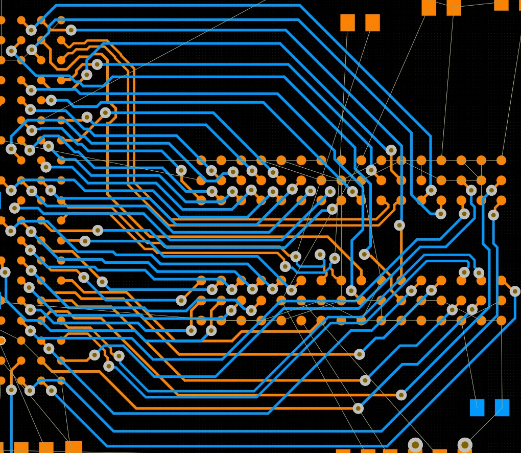
The standard 0.8mm-pitch BGAs that mostly make up this review have a coarse-enough pitch to allow a single trace to pass between two adjacent balls, as well as allowing a via to be placed in the middle of a 4-ball grid with enough room between adjacent vias to allow a track to go between them. This is illustrated in the image above on the left : notice that the inner-most signals on the blue (bottom) layer escape the BGA package by traveling between the vias used to escape the outer-most signals on the blue layer.
本文涉及的大部分芯片都是标准 0.8mm 间距的 BGA 封装, 具有足够粗的间距, 允许单条导线通过两个相邻焊盘之间, 同时允许在一个4焊球的网格中间放置一个过孔, 且相邻过孔之间有足够的空间以容纳导线通过. 这在上面的左图中有说明 : 注意蓝色层 (底层) 最里侧的信号在蓝色层最外侧信号使用的过孔之间传输而离开 BGA 封装.
In general, you can escape 4 rows of signals on a 0.8mm-pitch BGA with this strategy : the first two rows of signals from the BGA can be escaped on the component-side layer, while the next two rows of signals must be escaped on a second layer. If you need to escape more rows of signals, you’d need additional layers. IC designers are acutely aware of that; if an IC is designed for a 4-layer board (with two signal layers and two power planes) , only the outer 4 rows of balls will carry I/O signals. If they need to escape more signals, they can start selectively depopulating balls on the outside of the package — removing a single ball gives space for three or four signals to fit through.
通常, 你可以使用此策略在 0.8mm 间距的 BGA 上引出 4 行焊盘的信号 : BGA 的前两行信号可以在焊盘的同一层上引出, 而接下来的两行信号必须在另二层上跳过. 如果你需要跳过更多行信号, 则需要额外的层. IC 设计人员对此非常清楚;如果 IC 是为 4 层板 (带有两个信号层和两个电源平面) 设计的, 则只有外部的 4 行球会携带 I/O 信号. 如果他们需要跳过更多信号, 他们可以从封装外开始选择性去除焊盘——移除一个焊盘可以为三到四个信号腾出空间.
For 0.65mm-pitch BGAs (top right) , a via can still (barely) fit between four pins, but there’s not enough room for a signal to travel between adjacent vias; they’re just too close. That’s why almost all 0.65mm-pitch BGAs must have selective depopulations on the outside of the BGA. You can see the escape strategy in the image on the right is much less orderly — there are other constraints (diff pairs, random power nets, final signal destinations) that often muck this strategy up. I think the biggest annoyance with BGAs is that decoupling capacitors usually end up on the bottom of the board if you have to escape many of the signals, though you can squeeze them onto the top side if you bump up the number of layers on your board (many solder-down SOMs do this) .
对于 0.65mm 间距的 BGA (右上方) , 过孔仍然可以 (勉强) 放置在四个引脚之间, 但相邻过孔之间没有足够的空间容纳信号走线;它们距离太近了. 这就是为什么几乎所有的 0.65mm 间距 BGA 必须在 BGA 外侧进行选择性去除的原因. 你可以看到右侧图片中的逃逸策略更加杂乱——由于其他约束 (差分对、随机电源网、最终信号目标等) , 这个策略常常会被打乱. 我认为使用 BGA 时最大的麻烦是, 如果需要逃逸多个信号, 去耦电容器通常必须放在 PCB 的底层; 不过, 如果你增加板层数量, 也可以将它们挤到顶部 (许多焊接式 SOM 板会这样做)
Hand-assembling PCBs with these BGAs on them is a breeze. Because 0.8mm-pitch BGAs have such a coarse pitch, placement accuracy isn’t particularly important, and I’ve never once detected a short-circuit on a board I’ve soldered. That’s a far cry from 0.4mm-pitch (or even 0.5mm-pitch) QFPs, which routinely have minor short-circuits here and there — mostly due to poor stencil alignment. I haven’t had issues soldering 0.65mm-pitch BGAs, either, but I feel like I have to be much more careful with them.
手焊这些带有 BGA 的 PCB 非常容易. 由于 0.8mm 间距的 BGA 具有很大的间距, 放置精度并不特别重要, 我从未在焊接的板上检测到短路. 这与 0.4mm 间距 (甚至 0.5mm 间距) 的 QFP 很不一样, QFP 通常会有一些轻微的短路——大多是由于不良的钢网对齐. 我焊接 0.65mm 间距的 BGA 也没有问题, 但我感觉我必须对它们更加小心.
To actually solder the boards, if you have an electric cooktop (I like the Cuisineart ones ) , you can hot-plate solder boards with BGAs on them. I have a reflow oven, but I didn’t use it once during this review — instead, I hot-plate the top side of the board, flip it over, paste it up, place the passives on the back, and hit it with a bit of hot air. Personally, I wouldn’t use a hot-air gun to solder BGAs or other large components, but others do it all the time. The advantage to hot-plate soldering is that you can poke and nudge misbehaving parts into place during the reflow cycle. I also like to give my BGAs a small tap to force them to self-align if they weren’t already.
为了实际焊接这些电路板, 如果你有电磁炉 (我喜欢Cuisineart的这款 ) , 你可以用热板焊接带有 BGA 的电路板. 我有一个回流焊炉, 但在这次焊接中我一次也没用它——相反, 我用热板加热电路板的顶层, 翻转过来, 再涂上焊膏, 把被动元件放在背面, 然后用热风枪加热. 我个人不会用热风枪焊接 BGA 或其他大元件, 但其他人经常这么做. 热板焊接的优点是, 在回流过程期间, 你可以手动调节和推动那些不太听话的元件到正确位置. 我还喜欢给我的 BGA 稍微碰一下, 强制它们自对准, 如果它们还没有对准的话.
Multiple voltage domains#
多电压域
Microcontrollers are almost universally supplied with a single, fixed voltage (which might be regulated down internally) , while most microprocessors have a minimum of three voltage domains that must be supplied by external regulators : I/O (usually 3.3V) , core (usually 1.0-1.2V) , and memory (fixed for each technology — 1.35V for DDR3L, 1.5V for old-school DDR3, 1.8V for DDR2, and 2.5V for DDR) . There are often additional analog supplies, and some higher-performance parts might have six or more different voltages you have to supply.
微控制器基本上只需要单一的固定电压 (可能会在内部进行降压调节) , 而大多数微处理器至少有三个需要由外部稳压器供电的电压域: I/O 电压 (通常是 3.3V) 、核心电压 (通常是 1.0-1.2V) 和内存电压 (每种技术固定—DDR3L为1.35V, 老款DDR3为1.5V, DDR2为1.8V, DDR为2.5V) . 通常还会有额外的模拟电源, 某些高性能的微处理器可能需要六个或更多的不同电压供应.
While many entry-level parts can be powered by a few discrete LDOs or DC/DC converters, some parts have stringent power-sequencing requirements. Also, to minimize power consumption, many parts recommend using dynamic voltage scaling, where the core voltage is automatically lowered when the CPU idles and lowers its clock frequency.
虽然许多入门级部件可以通过几个 LDO 或 DC/DC 转换器供电, 但某些部件对电源时序有严格的要求. 此外, 为了最小化功耗, 许多芯片会建议使用动态电压调整, 当 CPU 空闲时自动降低核心电压并降低其时钟频率.
These two points lead designers to I2C-interfaced PMIC (power management integrated circuit) chips that are specifically tailored to the processor’s voltage and sequencing requirements, and whose output voltages can be changed on the fly. These chips might integrate four or more DC/DC converters, plus several LDOs. Many include multiple DC inputs along with built-in lithium-ion battery charging. Coupled with the large inductors, capacitors, and multiple precision resistors some of these PMICs require, this added circuitry can explode your bill of materials (BOM) and board area.
这两点引导设计师选择针对处理器电压和时序要求量身定制的 I2C 接口 PMIC (power management integrated circuit, 电源管理芯片) , 其输出电压可以即时更改. 这些芯片可能集成了四个或更多的 DC/DC 转换器, 以及多个 LDO. 许多芯片包括多个直流输入和内置锂离子电池充电功能. 结合这些 PMIC 所需的大电感、电容和多个精密电阻, 这种附加电路可能会让你的物料清单 (BOM) 和板面积大幅增加.
Regardless of your voltage regulator choices, these parts gesticulate wildly in their power consumption, so you’ll need some basic PDN design ability to ensure you can supply the parts with the current they need when they need it. And while you won’t need to do any simulation or verification just to get things to boot, if things are marginal, expect EMC issues down the road that would not come up if you were working with simple microcontrollers.
无论你选择什么样的电压调节器, 这些部件的功耗波动非常大, 因此你需要具备一些基本的 PDN (power distribution network, 电源分配网络) 设计能力, 以确保能够在需要时为这些部件提供足够的电流. 而且, 虽然仅仅为了启动系统, 你不需要进行任何仿真或验证, 但如果功耗边际不稳, 以后可能会遇到电磁兼容性 (EMC) 问题, 而这些问题在使用简单微控制器时通常不会出现.
Non-volatile storage#
非易失性存储器
No commonly-used microprocessor has built-in flash memory, so you’re going to need to wire something up to the MPU to store your code and persistent data. If you’ve used parts from fabless companies who didn’t want to pay for flash IP, you’ve probably gotten used to soldering down an SPI NOR flash chip, programming your hex file to it, and moving on with your life. When using microprocessors, there are many more decisions to consider.
没有常用的微处理器内置存储器, 因此你需要让 MPU 连接一些东西来存储代码和持久数据. 如果你使用了不想为闪存 IP 付费的无厂半导体公司生产的芯片, 你可能已经习惯了焊接 SPI NOR 闪存芯片, 将 hex 文件烧录到它上面, 然后再做别的. 在使用微处理器时, 需要考虑的决策要多得多.
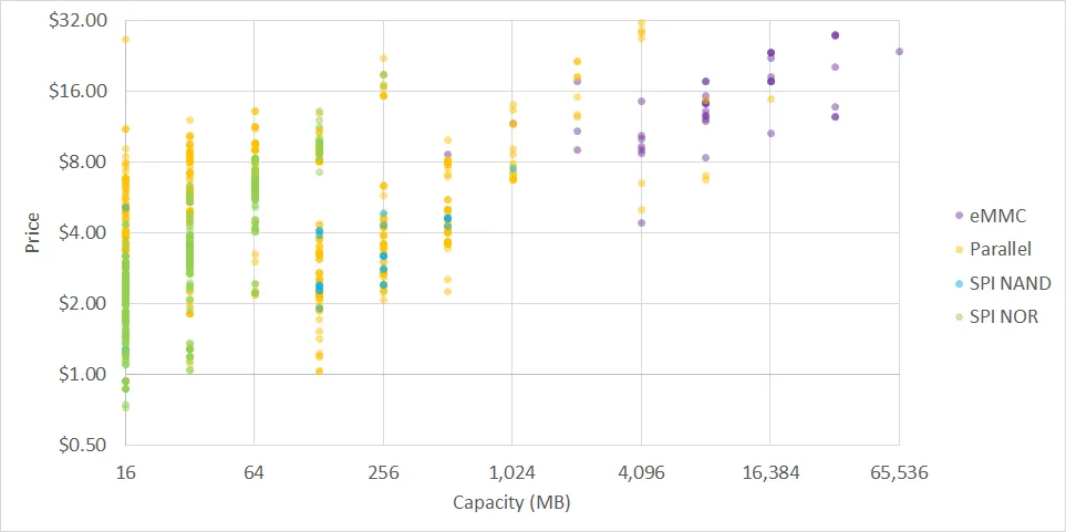
从 16MB 至 64GB 存储器在Digi-Key 上的价格,按存储器技术显示颜色
Most MPUs can boot from SPI NOR flash, SPI NAND flash, parallel, or MMC (for use with eMMC or MicroSD cards). Because of its organization, NOR flash memory has better read speeds but worse write speeds than NAND flash. SPI NOR flash memory is widely used for tiny systems with up to 16 MB of storage, but above that, SPI NAND and parallel-interfaced NOR and NAND flash become cheaper. Parallel-interfaced NOR flash used to be the ubiquitous boot media for embedded Linux devices, but I don’t see it deployed as much anymore — even though it can be found at sometimes half the price of SPI flash. My only explanation for its unpopularity is that no one likes wasting lots of I/O pins on parallel memory.
大多数 MPU 可以从 SPI NOR 闪存、SPI NAND 闪存、并行接口闪存或 MMC (用于 eMMC 或 MicroSD 卡)启动. 由于其架构, NOR 闪存内存的读取速度比 NAND 闪存好, 但写入速度差. SPI NOR 闪存内存广泛用于存储量小于 16MB 的小型系统, 但超过这个容量, SPI NAND 和并行接口的 NOR 和 NAND 闪存变得更便宜. 并行接口的 NOR 闪存曾经是嵌入式 Linux 设备的常用启动媒介, 但现在我很少看到有人用它——尽管它的价格有时只有 SPI 闪存的一半. 我对它不受欢迎的唯一解释是没有人喜欢在并行存储器上浪费大量的 I/O 引脚.
Above 1 GB, MMC is the dominant technology in use today. For development work, it’s especially hard to beat a MicroSD card — in low volumes they tend to be cheaper per gigabyte than anything else out there, and you can easily read and write to them without having to interact with the MPU’s USB bootloader; that’s why it was my boot media of choice on almost all platforms reviewed here. In production, you can easily switch to eMMC, which is, very loosely speaking, a solder-down version of a MicroSD card.
超过 1GB, MMC 是目前应用中的主导技术. 对于开发工作来说, 很难击败 MicroSD 卡——在低容量下, 它们每 GB 的价格通常比其他类型都要便宜, 并且你可以轻松地读写它们, 而无需与 MPU 的 USB 引导加载程序交互; 这就是为什么它几乎成为我在这里所有平台上的首选引导媒介. 在生产中, 你可以轻松切换到 eMMC, 简单来说, 它是一种焊接版本的 MicroSD 卡.
Booting#
启动
Back when parallel-interfaced flash memory was the only game in town, there was no need for boot ROMs: unlike SPI or MMC, these devices have address and data pins, so they are easily memory-mapped; indeed, older processors would simply start executing code straight out of parallel flash on reset.
当年并行接口闪存是市场上唯一的选择时, 无需启动 ROM. 它与 SPI 或 MMC 不同, 这些设备有地址和数据引脚, 因此它们很容易进行内存映射; 实际上, 较老的处理器会在复位时直接从并行闪存中执行代码.
That’s all changed though: modern application processors have boot ROM code baked into the chip to initialize the SPI, parallel, or SDIO interface, load a few pages out of flash memory into RAM, and start executing it. Some of these ROMs are quite fancy, actually, and can even load files stored inside a filesystem on an MMC device. When building embedded hardware around a part, you’ll have to pay close attention to how to configure this boot ROM.
不过, 这一切都改变了: 现代应用处理器将引导 ROM 代码嵌入到芯片中, 以初始化 SPI、并行或 SDIO 接口, 将一些页从闪存加载到 RAM 中, 并开始执行. 实际上, 其中一些 ROM 相当复杂, 甚至可以加载存储在 MMC 设备文件系统中的文件. 当围绕某个部件构建嵌入式硬件时, 你必须密切注意如何配置这个引导 ROM.
While some microprocessors have a basic boot strategy that simply tries every possible flash memory interface in a specified order, others have extremely complicated (“flexible”?) boot options that must be configured through one-time-programmable fuses or GPIO bootstrap pins. And no, we’re not talking about one or two signals you need to handle: some parts have more than 30 different bootstrap signals that must be pulled high or low to get the part booting correctly.
虽然一些微处理器有一个基本的引导策略, 简单地按照指定顺序尝试每个可能的闪存接口, 而另一些则具有极其复杂的 (“灵活的?”) 引导选项, 这些选项必须通过一次性可编程熔丝或 GPIO 引导引脚进行配置. 不, 我们不是在谈论你需要处理的一个或两个信号: 有些部件有超过 30 个不同的引导信号, 必须将其拉高或拉低才能正确引导启动.
Console UART#
控制台 UART
Unlike MCU-based designs, on an embedded Linux system, you absolutely, positively, must have a console UART available. Linux’s entire tracing architecture is built around logging messages to a console, as is the U-Boot bootloader.
与基于 MCU 的设计不同, 在嵌入式 Linux 系统中, 你绝对、肯定必须有一个可用的控制台 UART. Linux 的整个跟踪架构都是围绕将日志消息记录到控制台来构建的, U-Boot 引导加载程序也是如此.
That doesn’t mean you shouldn’t also have JTAG/SWD access, especially in the early stage of development when you’re bringing up your bootloader (otherwise you’ll be stuck with
printf()calls). Having said that, if you actually have to break out your J-Link on your embedded Linux board, it probably means you’re having a really bad day. While you can attach a debugger to an MPU, getting everything set up correctly is extremely clunky when compared to debugging an MCU. Prepare to relocate symbol tables as your code transitions from SRAM to main DRAM memory. It’s not uncommon to have to muck around with other registers, too (like forcing your CPU out of Thumb mode). And on top of that, I’ve found that some U-Boot ports remux the JTAG pins (either due to alternate functionality or to save power), and the JTAG chains on some parts are quite complex and require using less-commonly used pins and features of the interface. Oh, and since you have an underlying Boot ROM that executes first, JTAG adapters can screw that up, too.
那并不意味着你不需要有 JTAG/SWD, 尤其是在开发早期, 当你启动引导加载程序时 (否则你将陷入 printf() 调用的困境). 话虽如此, 如果你真的需要在你的嵌入式 Linux 板上断开 J-Link, 那可能意味着事情有点糟糕. 虽然你可以将调试器连接到 MPU, 但与调试 MCU 相比, 要把它们都设置好非常繁琐. 你要准备在代码从 SRAM 移动到主 DRAM 内存时重定位符号表. 你需要与其他寄存器 (如强制 CPU 退出 Thumb 模式) 纠缠的情况也不少见. 而且, 更重要的是, 我发现一些 U-Boot 端口重新配置了 JTAG 引脚 (要么是因为备用功能, 要么是为了省电), 某些部件的 JTAG 连接相当复杂, 需要使用较少使用的引脚和接口功能. 哦, 还有, 由于你有一个首先执行的底层 Boot ROM, JTAG 适配器也可能搞砸它.
Sidebar: Gatekeepers and the Myth of DDR Routing Complexity#
相关: 新手拦路虎与黑神话: DDR 布线
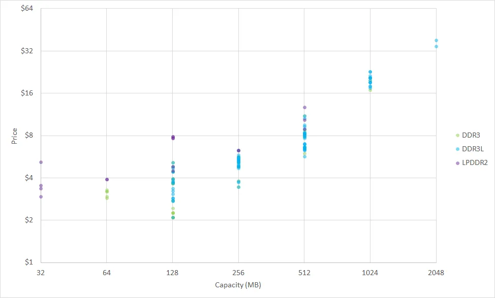
当前 Digi-Key 的价格趋势显示, 512 MB DDR3/DDR3L 内存性价比最高, 而单芯片 1 GB 和 2 GB 选项则需要支付 30% 的溢价.
If you start searching around the Internet, you’ll stumble upon a lot of posts from people asking about routing an SDRAM memory bus, only to be discouraged by “experts” lecturing them on how unbelievably complex memory routing is and how you need a minimum 6-layer stack-up and super precise length-tuning and controlled impedances and $200,000 in equipment to get a design working.
如果你在网上搜索, 你会发现很多人在问如何布线 SDRAM 内存总线, 但往往会被 “专家” 们关于内存布线如何不可思议地复杂、需要至少 6 层堆叠、超精确的长度调节、阻抗匹配以及需要 20 万美元的设备才能做好设计的说教所气馁.
That’s utter bullshit. In the grand scheme of things, routing memory is, at worst, a bit tedious. Once you’ve had some practice, it should take about an hour or so to route a 16-bit-wide single-chip DDR3 memory bus, so I’d hardly call it an insurmountable challenge. It’s worth investing a bit of time to learn about it since it will give you immense design flexibility when architecting your system (since you won’t be beholden to expensive SoMs or SiP-packaged parts).
那纯粹是胡说八道. 从大局来看, 给内存布线充其量是有点繁琐. 一旦你有些实践经验, 大约一个小时左右就能给一个 16 位宽的单芯片 DDR3 内存总线布好线, 所以我几乎不认为这是一个不可逾越的挑战. 花点时间去了解它是有价值的, 因为它在你构建系统时将给你带来极大的设计灵活性 (因为你不会依赖于昂贵的 SoM 或 SiP 封装部件).
Let’s get one thing straight: I’m not talking about laying out a 64-bit-wide quad-bank memory bus with 16 chips on an 8-layer stack-up. Instead, we’re focused on a single 16-bit-wide memory chip routed point-to-point with the CPU. This is the layout strategy you’d use with all the parts in this review, and it is drastically simpler than multi-chip layouts — no address bus terminations, complex T-topology routes, or fly-by write-leveling to worry about. And with modern dual-die DRAM packages, you can get up to 2 GB capacity in a single DDR3L chip. In exchange for the markup you’ll pay for the dual-die chips, you’ll end up with much easier PCB routing.
让我们明确一点: 我说的不是在 8 层板上给一个有 16 个芯片的 64 位宽的四通道内存总线 layout. 相反, 我们专注于一个单 16 位宽的内存芯片, 与 CPU 进行点对点连接. 这是你在这次评测中所有部件都会使用的布局策略, 它比多芯片布局简单得多——无需考虑地址总线终端电阻、复杂的 T 拓扑或 fly-by 拓扑时的 write-leveling. 而且, 使用现代的双芯片堆叠 DRAM 封装, 你可以在单颗 DDR3L 芯片中实现最高 2GB 的容量. 虽然你需要为双芯片封装支付额外费用, 但换来的却是极大简化的PCB布线.
Length Tuning#
长度调节
When most people think of DDR routing, length-tuning is the first thing that comes to mind. If you use a decent PCB design package, setting up length-tuning rules and laying down meandered routes is so trivial to do that most designers don’t think anything of it — they just go ahead and length-match everything that’s relatively high-speed — SDRAM, SDIO, parallel CSI / LCD, etc. Other than adding a bit of design time, there’s no reason not to maximize your timing margins, so this makes sense.
当大多数人想到 DDR 布线时, 首先想到的是长度调节. 如果你使用一个不错的 PCB 设计软件, 设置长度调节规则和绘制蛇形线会变得很简单以至于很多设计师都不会怎么管——他们只要继续画就行了, 将所有相对高速的部件进行长度匹配——SDRAM、SDIO、并行 CSI / LCD 等. 除了增加一点设计时间外, 没有理由不最大化你的时序余量, 因此这很有道理。
But what if you’re stuck in a crappy software package, manually exporting spreadsheets of track lengths, manually determining matching constraints, and — gasp — maybe even manually creating meanders? Just how important is length-matching? Can you get by without it?
但是, 如果你不得不用一个糟糕的软件, 手动导出轨道长度的电子表格, 手动确定匹配约束, 甚至——天哪——可能还需要手画蛇形线? 长度匹配很重要吗? 没有它可以吗?
Most microprocessors reviewed here top out at DDR3-800, which has a bit period of 1250 ps. Slow DDR3-800 memory might have a data setup time of up to 165 ps at AC135 levels, and a hold time of 150 ps. There’s also a worst-case skew of 200 ps. Let’s assume our microprocessor has the same specs. That means we have 200 ps of skew from our processor + 200 ps of skew from our DRAM chip + 165 ps setup time + 150 ps of hold time = 715 ps total. That leaves a margin of 535 ps (more than 3500 mil!) for PCB length mismatching.
大多数本文讲到的微处理器最高支持 DDR3-800, 其位周期为 1250 ps. 慢速 DDR3-800 内存可能在 AC135 水平下具有高达 165 ps 的数据设置时间, 以及 150 ps 的保持时间. 还有 200 ps 的最坏情况偏移. 假设我们的微处理器具有相同的规格. 这意味着我们从处理器那里有 200 ps 的偏移 + 从我们的 DRAM 芯片那里有 200 ps 的偏移 + 165 ps 的设置时间 + 150 ps 的保持时间 = 总共 715 ps. 这留下了 535 ps 的余量 (超过 3500 mil! )用于 PCB 长度不匹配.
i.MX 6UL 的修订历史显示, 恩智浦实际上移除了 DDR 内存控制器的时序参数
Are our assumptions about the MPU’s memory controller valid? Who knows. One issue I ran into is that there’s a nebulous cloud surrounding the DDR controllers on many application processors. Take the i.MX 6UL as an example: I discovered multiple posts where people add up worst-case timing parameters in the datasheet, only to end up with practically no timing margin. These official datasheet numbers seem to be pulled out of thin air — so much so that NXP literally removed the entire DDR section in their datasheet and replaced it with a boiler-plate explanation telling users to follow the “hardware design guidelines.” Texas Instruments and ST also lack memory controller timing information in their documentation — again, referring users to stringent hardware design rules. ((Rockchip and Allwinner don’t specify any sort of timing data or length-tuning guidelines for their processors at all.))
我们的对 MPU 内存控制器的假设是否有效? 谁知道呢. 我的一个问题是, 许多应用处理器的 DDR 控制器是个迷. 以 i.MX 6UL 为例: 我发现有好多篇帖子, 他们在数据手册中累加最坏情况下的时序参数, 结果实际上几乎没有时序余量. 这些官方数据手册中的数字似乎是随意的——太多了, 以至于后来 NXP 在他们的数据手册删除了整个 DDR 部分, 并用一个模板化的解释替换, 告诉用户遵循 “硬件设计指南”. 德州仪器和 ST 也在他们的文档中缺乏内存控制器时序信息, 也用严格的硬件设计规则指引用户. (Rockchip 和 Allwinner 甚至没有为其处理器指定任何类型的时序数据或长度调节指南.)
How stringent are these rules? Almost all of these companies recommend a ±25-mil match on each byte group. Assuming 150 ps/cm propagation delay, that’s ±3.175 ps — only 0.25% of that 1250ps DDR3-800 bit period. That’s absolutely nuts. Imagine if you were told to ensure your breadboard wires were all within half an inch in length of each other before wiring up your Arduino SPI sensor project — that’s the equivalent timing margin we’re talking about.
这些规则有多严格? 几乎所有这些公司都建议每个字节组匹配 ±25-mil. 假设 150 ps/cm 的传播延迟, 那就是 ±3.175 ps——仅占 1250ps DDR3-800 位周期的 0.25%. 这绝对是疯了. 就像有人告诉你要在焊接 Arduino SPI 传感器项目之前确保面包板上的所有电线长度都在半英寸以内——这就是我们所说的时序容限.
To settle this, I empirically tested two DDR3-800 designs — one with and one without length tuning — and they performed identically. In neither case was I ever able to get a single bit error, even after thousands of iterations of memory stress-tests. Yes, that doesn’t prove that the design would run for 24/7/365 without a bit error, but it’s definitely a start. Just to verify I wasn’t on the margin, or that this was only valid for one processor, I overclocked a second system’s memory controller by two times — running a DDR3-800 controller at DDR3-1600 speeds — and I was still unable to get a single bit error. In fact, all five of my discrete-SDRAM-based designs violated these length-matching guidelines and all five of them completed memory tests without issue, and in all my other testing, I never experienced a single crash or lock-up on any of these boards.
为了解决这个问题, 我经验性地测试了两种 DDR3-800 设计——一种带有长度调节, 一种不带——它们的表现完全相同. 在两种情况下, 即使经过数千次迭代的内存压力测试, 我都没有得到一个比特的错误. 是的, 这并不证明该设计可以在 24/7/365 不间断运行而不出现单比特错误, 但这确实是一个开始. 为了验证我并没有处于临界情况, 或者这不仅仅适用于一个处理器, 我将第二块板的内存控制器超频了两倍——以 DDR3-1600 的速度运行 DDR3-800 控制器——我仍然无法得到一个比特的错误. 事实上, 我的五个分立 SDRAM 的设计都违反了这些长度匹配指南, 但它们都完成了内存测试而没有问题, 在我所有的其他测试中, 我也从未在这些板子上经历过任何崩溃或锁定.
My take-away: length-tuning is easy if you have good CAD software, and there’s no reason not to spend an extra 30 minutes length-tuning things to maximize your timing budget. But if you use crappy CAD software or you’re rushing to get a prototype out the door, don’t sweat it — especially for Rev A.
我的体会: 如果你有好的 CAD 软件, 长度调节很容易, 多花 30 分钟来调整长度的时间也没什么. 但如果你使用的是糟糕的 CAD 软件或者你急于推出原型, 那就别担心了——尤其是对于初步样板.
More importantly, a corollary: if your design doesn’t work, length-tuning is probably the last thing you should be looking at. For starters, make sure you have all the pins connected properly — even if the failures appear intermittent. For example, accidentally swapping byte lane strobes / masks (like I’ve done) will cause 8-bit operations to fail without affecting 32-bit operations. Since the bulk of RAM accesses are 32-bit, things will appear to kinda-sorta work.
更重要的是一个推论: 如果你的设计不能正常工作, 长度调节可能是你应该考虑的最后一件事. 首先, 确保你已经正确连接了所有引脚——即使故障是间歇性的. 例如, 意外交换字节通道选通/掩码 (就像我做过的那样) 会导致 8 位操作失败, 而不会影响 32 位操作. 由于大部分 RAM 访问都是 32 位的, 它看起有点像正常工作的样子.
Signal Integrity#
信号完整性
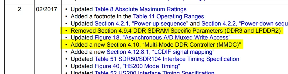
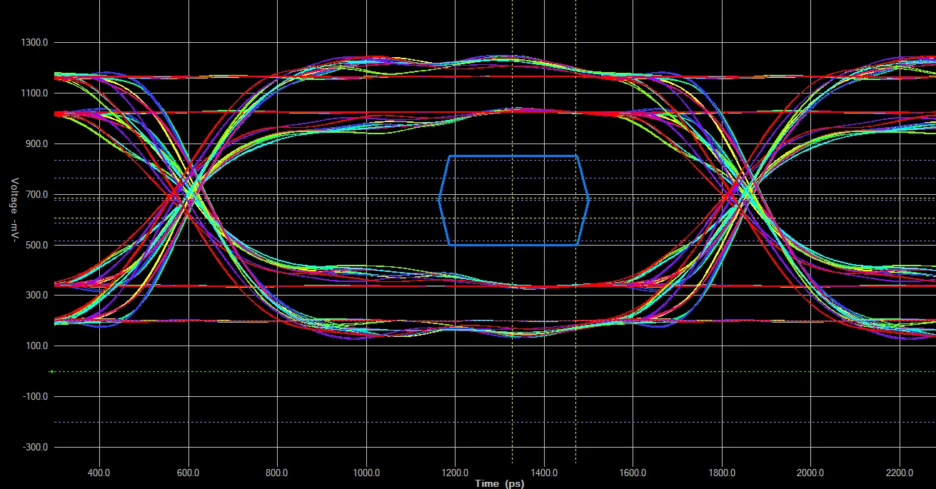
这张眼图显示了一个经过严格长度调节的单个数据组, 但信号完整性较差. 绿色的信号表示从 DRAM 芯片的裸片上看到的选通信号. 蓝色的眼表示 DDR3L 内存在 DDR3-800 工作时, 围绕时钟过渡点的 AC175 电平设置和保持时间.
Instead of worrying about length-tuning, if a design is failing (either functionally or in the EMC test chamber), I would look first at power distribution and signal integrity. I threw together some HyperLynx simulations of various board designs with different routing strategies to illustrate some of this. I’m not an SI expert, and there are better resources online if you want to learn more practical techniques; for more theory, the books that everyone seems to recommend are by Howard Johnson: High Speed Digital Design: A Handbook of Black Magic and High Speed Signal Propagation: Advanced Black Magic, though I’d also add Henry Ott’s Electromagnetic Compatibility Engineering book to that list.
设计失败时, 不管是功能上还是 EMC 测试, 相比担心长度调节, 我会首先检查电源分配和信号完整性. 我针对不同布线策略的多种板级设计进行了 HyperLynx 模拟, 以说明其中的一些内容. 我不是 SI 专家, 如果你想要学习更多实用技术, 网上有更好的资源; 对于理论, 大家似乎都推荐霍华德·约翰逊的书:《高速数字设计: 黑魔法手册》和《高速信号传播: 高级黑魔法》, 但我也会推荐亨利·奥特的《电磁兼容性工程》这本书.
Ideally, every signal’s source impedance, trace impedance, and load impedance would match. This is especially important as a trace’s length starts to approach the wavelength of the signal (I think the rule of thumb is 1/20th the wavelength), which will definitely be true for 400 MHz and faster DDR layouts.
理想情况下, 每个信号的源阻抗、走线阻抗和负载阻抗应匹配. 这对于走线长度开始接近信号波长的情况 (我的经验法则是波长的 1/20) 尤为重要, 这对于 400 MHz 和更快的 DDR 布局肯定成立。
Using a proper PCB stack-up (usually a ~0.1mm prepreg will result in a close-to-50-ohm impedance for a 5mil-wide trace) is your first line of defense against impedance issues, and is usually sufficient for getting things working well enough to avoid simulation / refinement.
使用合适的 PCB 叠层 (通常 0.1mm 预浸料可以使 5mil 宽的走线接近 50 欧姆阻抗) 是你对抗阻抗问题的第一道防线, 通常足以使电路运行良好, 以避免仿真/优化.
For the data groups, DDR3 uses on-die termination (ODT), configurable for 40, 60, or 120 ohm on memory chips (and usually the same or similar on the CPU) along with adjustable output impedance drivers. ODT is only enabled on the receiver’s end, so depending on whether you’re writing data or reading data, ODT will either be enabled on the memory chip, or on the CPU.
对于数据组, DDR3 使用片上终端电阻 (on-die termination, ODT), 可以在内存芯片上配置为 40 欧姆、60 欧姆或1 20 欧姆 (通常在 CPU 端也类似). 此外, 还支持可调的输出阻抗驱动器. ODT 只在接收端启用, 因此, 根据是写数据还是读数据, ODT 会分别启用在内存芯片或 CPU 上.
For simple point-to-point routing, don’t worry too much about ODT settings. As can be seen in the above eye diagram, the difference between 33-ohm and 80-ohm ODT terminations on a CPU reading from DRAM is perceivable, but both are well within AC175 levels (the most stringent voltage levels in the DDR3 spec). The BSP for your processor will initialize the DRAM controller with default settings that will likely work just fine.
对于简单的点对点布线, 无需过分关注 ODT 设置. 如上面的眼图所示, 在从 DRAM 读取的 CPU 上, 33 欧姆和 80 欧姆 ODT 之间的差异是可感知的, 但两者都很好地处在 AC175 级别 (DDR3 规范中最严格的电压级别) 之内. 你的处理器的 BSP 使用默认设置初始化 DRAM 控制器, 这些设置很可能工作得很好.
未配备终端电阻的地址总线, 通过慢速上升沿/下降沿时间设置和 80 欧姆输出驱动器调整到了这样. 存在明显的过冲, 但小于 DRAM 数据手册中的 400mV 规格. 信号间的偏移来自近 300mil 的长度不匹配.
The biggest source of EMC issues related to DDR3 is likely going to come from your address bus. DDR3 uses a one-way address bus (the CPU is always the transmitter and the memory chip is always the receiver), and DDR memory chips do not have on-chip termination for these signals. Theoretically, they should be terminated to VTT (a voltage derived from VDDQ/2) with resistors placed next to the DDR memory chip. On large fly-by buses with multiple memory chips, you’ll see these VTT termination resistors next to the last chip on the bus. The resistors absorb the EM wave propagating from the MPU which reduces the reflections back along the transmission line that all the memory chips would see as voltage fluctuations. On small point-to-point designs, the length of the address bus is usually so short that there’s no need to terminate. If you run into EMC issues, consider software fixes first, like using slower slew-rate settings or increasing the output impedance to soften up your signals a bit.
与 DDR3 相关的 EMC 问题最大的来源可能是地址总线. DDR3 使用单向地址总线 (CPU 始终是发送方, 内存芯片始终是接收方), 并且 DDR 内存芯片对于这些信号没有片上终端电阻. 理论上, 这些信号应该通过靠近 DDR 内存芯片放置的电阻连接到 VTT (从 VDDQ/2 导出的电压). 在包含多个内存芯片的大型 fly-by 总线中, 这些 VTT 终端电阻通常位于总线上最后一个内存芯片旁边. 电阻会吸收从 MPU 传来的电磁波, 减少沿传输线反射回来的信号, 这种反射会导致所有内存芯片检测到电压波动. 在小型点对点设计中, 地址总线通常很短, 不需要终端电阻. 如果遇到 EMC 问题, 可以首先尝试通过软件解决, 比如使用较慢的上升沿/下降沿时间设置或增加输出阻抗以稍微平滑信号.
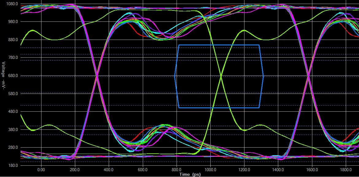
我们可以通过在信号之间留出大量间距来降低串扰, 但对于单芯片 DRAM 布线来说, 这通常是多余的, 因为走线长度通常小于 2 英寸.
Another source of SI issues is cross-coupling between traces. To reduce cross-talk, you can put plenty of space between traces — three times the width (3S) is a standard rule of thumb. I sound like a broken record, but again, don’t be too dogmatic about this unless you’re failing tests, as the lengths involved with routing a single chip are so short. The above figure illustrates the routing of a DDR bus with no length-tuning but with ample space between traces. Note the eye diagram (below) shows much better signal integrity (at the expense of timing skew) than the first eye diagram presented in this section.
另一个 SI 问题来源是传输线之间的串扰。为了减少串扰,你可以它们之间留出足够的间距——按标准通常是宽度的三倍 (3S). 虽然有点婆婆妈妈, 但我还是要强调, 除非你在测试中失败, 否则不要对此过于教条, 因为单芯片布线涉及的长度非常短. 上图展示了没有长度调节但传输线之间有足够空间的 DDR 总线布线. 下面的眼图比本节中首次展示的第一个眼图具有更好的信号完整性 (以牺牲时序偏移为代价).
按 3S 规则布线的内存总线的眼图. 在 50 欧姆微带线使用 40 欧姆输出时, 使用 33 欧姆和 80 欧姆 ODT 终端的区别. 两者都完全符合严格的 AC175 规范, 但 80 欧姆的过冲和振荡更明显, 而 30 欧姆则过度阻尼. 信号偏斜是短信号和长信号之间 150mil 长度差异的结果.
Pin Swapping#
引脚交换
Because DDR memory doesn’t care about the order of the bits getting stored, you can swap individual bits — except the least-significant one if you’re using write-leveling — in each byte lane with no issues. Byte lanes themselves are also completely swappable. Having said that, since all the parts I reviewed are designed to work with a single x16-wide DDR chip (which has an industry-standard pinout), I found that most pins were already balled out reasonably well. Before you start swapping pins, make sure you’re not overlooking an obvious layout that the IC designers intended.
因为 DDR 内存不关心存储的位顺序, 所以你可以交换每个字节通道中的单个位 (如果你使用写均衡,则不包括最低有效位) 而不会出现任何问题. 字节通道本身也可以完全交换. 话虽如此, 由于我审查的所有部件都是为与单个 x16 宽的 DDR 芯片 (具有行业标准引脚配置) 一起工作而设计的, 我发现大多数引脚已经相当合理地焊接好了. 在你交换引脚之前, 确保你没有忽略 IC 设计者有意设计的布局.
Recommendations#
建议
Instead of worrying about chatter you read on forums or what the HyperLynx salesperson is trying to spin, for simple point-to-point DDR designs, you shouldn’t have any issues if you follow these suggestions:
不用担心你在论坛上看到的闲言碎语, 或者 HyperLynx 销售员试图推销的内容, 对于简单的点对点 DDR 设计, 如果你遵循以下建议, 你就不会有任何问题:
Pay attention to PCB stack-up. Use a 4-layer stack-up with thin prepreg (~0.1mm) to lower the impedance of your microstrips — this allows the traces to transfer more energy to the receiver. Those inner layers should be solid ground and DDR VDD planes respectively. Make sure there are no splits under the routes. If you’re nit-picky, pull back the outer-layer copper fills from these tracks so you don’t inadvertently create coplanar structures that will lower the impedance too much.
注意 PCB 叠层. 使用 4 层堆叠, 并采用薄预浸料 (约 0.1mm) 以降低微带线的阻抗——这允许传输线将更多能量传输到接收端. 那些内部层应该是完整的接地层和 DDR VDD 平面. 确保走线下方没有任何分割. 如果追求细节, 可以将外层的铜填充从这些信号线附近撤离, 避免无意间形成共面结构, 从而导致阻抗过低.
Avoid multiple DRAM chips. If you start adding extra DRAM chips, you’ll have to route your address/command signals with a fly-by topology (which requires terminating all those signals — yuck), or a T-topology (which requires additional routing complexity). Stick with 16-bit-wide SDRAM, and if you need more capacity, spend the extra money on a dual-die chip — you can get up to 2 GB of RAM in a single X16-wide dual-rank chip, which should be plenty for anything you’d throw at these CPUs.
避免使用多个DRAM芯片. 如果添加额外的DRAM芯片, 你将不得不为地址和命令信号采用 fly-by 拓扑 (这需要对所有这些信号进行终端匹配——麻烦得很), 或者采用 T 型拓扑 (这会带来额外的布线复杂性). 建议使用 16 位宽的 SDRAM. 如果需要更大的容量, 可以多花一些钱购买双模封装的芯片——单个 16 位宽、双排 (dual-rank) 的芯片可以提供高达 2GB 的容量, 这对这些 CPU 来说已经绰绰有余了.
Faster RAM makes routing easier. Even though our crappy processors reviewed here rarely can go past 400-533 MHz DDR speeds, using 800 or 933 MHz DDR chips will ease your timing budget. The reduced setup/hold times make address/command length-tuning almost entirely unnecessary, and the reduced skew even helps with the bidrectional data bus signals.
更快的 RAM 让布线变得更简单. 尽管我们在这里讨论的低性能处理器很难超过 400-533 MHz DDR 的速度, 但使用 800 或 933 MHz 的 DDR 芯片反而能让时间预算变得宽松. 更短的建立时间和保持时间几乎让地址/命令信号的长度调谐变得完全不必要, 而且更低的偏移甚至对双向数据总线信号也有帮助.